 |
| December 03, 2019 | Volume 15 Issue 46 |
Electrical/Electronic News & Products
Designfax weekly eMagazine

Archives
Partners
Manufacturing Center
Product Spotlight
Modern Applications News
Metalworking Ideas For
Today's Job Shops
Tooling and Production
Strategies for large
metalworking plants
Intro to reed switches, magnets, magnetic fields
 This brief introductory video on the DigiKey site offers tips for engineers designing with reed switches. Dr. Stephen Day, Ph.D. from Coto Technology gives a solid overview on reed switches -- complete with real-world application examples -- and a detailed explanation of how they react to magnetic fields.
View the video.
Bi-color LEDs to light up your designs
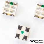 Created with engineers and OEMs in mind, SpectraBright Series SMD RGB and Bi-Color LEDs from Visual Communi-cations Company (VCC) deliver efficiency, design flexibility, and control for devices in a range of industries, including mil-aero, automated guided vehicles, EV charging stations, industrial, telecom, IoT/smart home, and medical. These 50,000-hr bi-color and RGB options save money and space on the HMI, communicating two or three operating modes in a single component.
Learn more.
All about slip rings: How they work and their uses
 Rotary Systems has put together a really nice basic primer on slip rings -- electrical collectors that carry a current from a stationary wire into a rotating device. Common uses are for power, proximity switches, strain gauges, video, and Ethernet signal transmission. This introduction also covers how to specify, assembly types, and interface requirements. Rotary Systems also manufactures rotary unions for fluid applications.
Read the overview.
Seifert thermoelectric coolers from AutomationDirect
 Automation-Direct has added new high-quality and efficient stainless steel Seifert 340 BTU/H thermoelectric coolers with 120-V and 230-V power options. Thermoelectric coolers from Seifert use the Peltier Effect to create a temperature difference between the internal and ambient heat sinks, making internal air cooler while dissipating heat into the external environment. Fans assist the convective heat transfer from the heat sinks, which are optimized for maximum flow.
Learn more.
EMI shielding honeycomb air vent panel design
 Learn from the engineering experts at Parker how honeycomb air vent panels are used to help cool electronics with airflow while maintaining electromagnetic interference (EMI) shielding. Topics include: design features, cell size and thickness, platings and coatings, and a stacked design called OMNI CELL construction. These vents can be incorporated into enclosures where EMI radiation and susceptibility is a concern or where heat dissipation is necessary. Lots of good info.
Read the Parker blog.
What is 3D-MID? Molded parts with integrated electronics from HARTING
 3D-MID (three-dimensional mechatronic integrated devices) technology combines electronic and mechanical functionalities into a single, 3D component. It replaces the traditional printed circuit board and opens up many new opportunities. It takes injection-molded parts and uses laser-direct structuring to etch areas of conductor structures, which are filled with a copper plating process to create very precise electronic circuits. HARTING, the technology's developer, says it's "Like a PCB, but 3D." Tons of possibilities.
View the video.
Loss-free conversion of 3D/CAD data
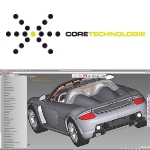 CT CoreTech-nologie has further developed its state-of-the-art CAD converter 3D_Evolution and is now introducing native interfaces for reading Solidedge and writing Nx and Solidworks files. It supports a wide range of formats such as Catia, Nx, Creo, Solidworks, Solidedge, Inventor, Step, and Jt, facilitating smooth interoperability between different systems and collaboration for engineers and designers in development environments with different CAD systems.
Learn more.
Top 5 reasons for solder joint failure
 Solder joint reliability is often a pain point in the design of an electronic system. According to Tyler Ferris at ANSYS, a wide variety of factors affect joint reliability, and any one of them can drastically reduce joint lifetime. Properly identifying and mitigating potential causes during the design and manufacturing process can prevent costly and difficult-to-solve problems later in a product lifecycle.
Read this informative ANSYS blog.
Advanced overtemp detection for EV battery packs
 Littelfuse has introduced TTape, a ground-breaking over-temperature detection platform designed to transform the management of Li-ion battery systems. TTape helps vehicle systems monitor and manage premature cell aging effectively while reducing the risks associated with thermal runaway incidents. This solution is ideally suited for a wide range of applications, including automotive EV/HEVs, commercial vehicles, and energy storage systems.
Learn more.
Benchtop ionizer for hands-free static elimination
 EXAIR's Varistat Benchtop Ionizer is the latest solution for neutralizing static on charged surfaces in industrial settings. Using ionizing technology, the Varistat provides a hands-free solution that requires no compressed air. Easily mounted on benchtops or machines, it is manually adjustable and perfect for processes needing comprehensive coverage such as part assembly, web cleaning, printing, and more.
Learn more.
LED light bars from AutomationDirect
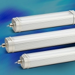 Automation-Direct adds CCEA TRACK-ALPHA-PRO series LED light bars to expand their offering of industrial LED fixtures. Their rugged industrial-grade anodized aluminum construction makes TRACKALPHA-PRO ideal for use with medium to large-size industrial machine tools and for use in wet environments. These 120 VAC-rated, high-power LED lights provide intense, uniform lighting, with up to a 4,600-lumen output (100 lumens per watt). They come with a standard bracket mount that allows for angle adjustments. Optional TACLIP mounts (sold separately) provide for extra sturdy, vibration-resistant installations.
Learn more.
World's first metalens fisheye camera
 2Pi Optics has begun commercial-ization of the first fisheye camera based on the company's proprietary metalens technology -- a breakthrough for electronics design engineers and product managers striving to miniaturize the tiny digital cameras used in advanced driver-assistance systems (ADAS), AR/VR, UAVs, robotics, and other industrial applications. This camera can operate at different wavelengths -- from visible, to near IR, to longer IR -- and is claimed to "outperform conventional refractive, wide-FOV optics in all areas: size, weight, performance, and cost."
Learn more.
Orbex offers two fiber optic rotary joint solutions
 Orbex Group announces its 700 Series of fiber optic rotary joint (FORJ) assemblies, supporting either single or multi-mode operation ideal for high-speed digital transmission over long distances. Wavelengths available are 1,310 or 1,550 nm. Applications include marine cable reels, wind turbines, robotics, and high-def video transmission. Both options feature an outer diameter of 7 mm for installation in tight spaces. Construction includes a stainless steel housing.
Learn more.
Mini tunnel magneto-resistance effect sensors
 Littelfuse has released its highly anticipated 54100 and 54140 mini Tunnel Magneto-Resistance (TMR) effect sensors, offering unmatched sensitivity and power efficiency. The key differentiator is their remarkable sensitivity and 100x improvement in power efficiency compared to Hall Effect sensors. They are well suited for applications in position and limit sensing, RPM measurement, brushless DC motor commutation, and more in various markets including appliances, home and building automation, and the industrial sectors.
Learn more.
Panasonic solar and EV components available from Newark
 Newark has added Panasonic Industry's solar inverters and EV charging system components to their power portfolio. These best-in-class products help designers meet the growing global demand for sustainable and renewable energy mobility systems. Offerings include film capacitors, power inductors, anti-surge thick film chip resistors, graphite thermal interface materials, power relays, capacitors, and wireless modules.
Learn more.
Beyond Moore's Law: Researchers take transistor arrays into the third dimension
Silicon integrated circuits, which are used in computer processors, are approaching the maximum feasible density of transistors on a single chip -- at least in two-dimensional arrays.
Now, a team of engineers at the University of Michigan (U-M) has stacked a second layer of transistors directly atop a state-of-the-art silicon chip.
They propose that their design could remove the need for a second chip that converts between high- and low-voltage signals, which currently stands between the low-voltage processing chips and the higher-voltage user interfaces.
"Our approach can achieve better performance in a smaller, lighter package," said Becky Peterson, an associate professor of electrical engineering and computer science and project leader.
Moore's Law holds that computing power per dollar doubles roughly every two years. As silicon transistors have shrunk in size to become more affordable and power efficient, the voltages at which they operate have also fallen.
Higher voltages would damage the increasingly small transistors. Because of this, state-of-the-art processing chips aren't compatible with higher-voltage user interface components, such as touchpads and display drivers. These need to run at higher voltages to avoid effects such as false touch signals or too-low brightness settings.
"To solve this problem, we're integrating different types of devices with silicon circuits in 3D, and those devices allow you to do things that the silicon transistors can't do," Peterson said.
Because the second layer of transistors can handle higher voltages, they essentially give each silicon transistor its own interpreter for talking to the outside world. This gets around the current tradeoff of using state-of-the-art processors with an extra chip to convert signals between the processor and interface devices -- or using a lower-grade processor that runs at a higher voltage.
"This enables a more compact chip with more functionality than what is possible with only silicon," said Youngbae Son, the first author of the paper and recent doctoral graduate in electrical and computer engineering at U-M.
Peterson's team managed this by using a different kind of semiconductor, known as an amorphous metal oxide. To apply this semiconductor layer to the silicon chip without damaging it, they covered the chip with a solution containing zinc and tin and spun it to create an even coat.
Next, they baked the chip briefly to dry it. They repeated this process to make a layer of zinc-tin-oxide about 75 nanometers thick -- about one-thousandth the thickness of a human hair. During a final bake, the metals bonded to oxygen in the air, creating a layer of zinc-tin-oxide.
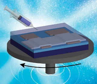
An illustration of a step in the production process, injecting the zinc-tin-solution atop the spinning silicon chip. [Image credit: Youngbae Son and Rose Anderson, Peterson Lab]
The team used the zinc-tin-oxide film to make thin film transistors. These transistors could handle higher voltages than the silicon beneath. Then, the team tested the underlying silicon chip and confirmed that it still worked.
To make useful circuits with the silicon chip, the zinc-tin-oxide transistors needed to fully communicate with the underlying silicon transistors. The team accomplished this by adding two more circuit elements using the zinc-tin-oxide: a vertical thin film diode and a Schottky-gated transistor.
The two kinds of zinc-tin-oxide transistors are connected together to make an inverter, converting between the low voltage used by the silicon chip and the higher voltages used by other components. The diodes were used to convert wireless signals into useful DC power for the silicon transistors.
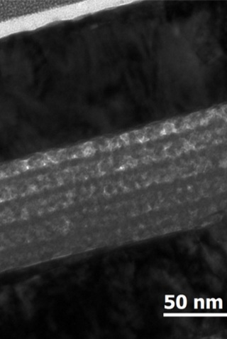
The zinc-tin-oxide semiconductor appears as five mottled gray layers in this electron microscope image. [Image credit: Youngbae Son, Peterson Lab]
These demonstrations pave the way toward silicon integrated circuits that go beyond Moore's law, bringing the analog and digital advantages of oxide electronics to individual silicon transistors.
The study was funded by a Defense Advanced Research Projects Agency (DARPA) Young Faculty Award.
Source: University of Michigan
Published December 2019
Rate this article
View our terms of use and privacy policy